In this chapter, we examined the requirements of the Microprocessor Unit (MPU) to communicate with memory and I/O devices and to process binary data. Based on those requirements, we designed a generalized model of the
M PU. We discussed memory in terms of its storage elements, namely, latches and registers and techniques of assigning addresses. The steps required for the MPU to communicate with memory and I/Os were briefly described. The important concepts are summarized as follows.
· The MPU performs four primary operations: Memory Read, Memory Write, I/O Read, and I/O Write.
· To communicate with memory and I/Os, the MPU needs three types of buses: the unidirectional address bus to send memory and I/O addresses, the bidirectional data bus to transfer data, and control signals to enable the devices.
· The MPU should have signal lines to accept and to acknowledge external requests. These requests are Reset (go back to beginning), interrupt ( stop the ongoing process and attend to something urgent). wait to synchronize with slow memory, and allow the use of buses to an external device because the MPU response time is slower than that of the external device.
· To process data, the MPU should include registers to store data, memory pointers to hold memory addresses, ALU to perform arithmetic and logic operations, and flags to indicate data conditions.
· Memory is a group of registers, arranged in a sequence, to store bits. The number of cells (latches) in a register determines the size of the memory word in a chip.
· A memory chip requires address lines to identify a memory register, Chip Select signal to select the chip, and control signals to read from and write into memory registers.
· The range of memory addresses assigned to a memory chip is done through
· the Chip Select logic.
· An I/O device can be identified either with an 8-bit address called the peripheral-mapped I/O or with a 16-bit address called the memory-mapped I/O.
· To communicate with memory or I/O, the MPU places the address of the device on the address bus, sends the appropriate control signal, and places (or receives) data on the data bus.
In this topic , we examined the microprocessor as a programmable logic device and developed a generalized model. Similarly, we discussed memory as a storage element and constructed a memory model. We examined briefly the role of l/Os as channels of communication with "the outside world." These three elements were interconnected through a bus architecture to form a model of a microprocessor-based system. Then we discussed how the MPU communicates with memory and I/Os.
In the next three chapters, we will explore each component and its communication process separately with details and specific examples. In Chapter 3. we will examine the Z80 microprocessor in the context of our generalized model of a programmable logic device. Chapter 4 discusses memory and its interfacing. and Chapter 5 is devoted to interfacing I/O devices.
1. List the four operations commonly performed by the MPU .
2. What is a bus?
3. What is the function of the address bus?
4. How many memory locations can be addressed by the MPU with thirteen address lines?
S. How many address lines are necessary to address two megabytes (2048K) of memory?
6. What is the function of the interrupt signal and when is it used?
7. When is the bus request signal used?
8. Specify the number of registers and memory cells in a 128 x 4 memory chip.
9. How many bits are stored by a 256 x 4 memory chip? Can this chip be specified as 128-byte memory?
10. If the memory size is 1024 x 4 bits, how many chips are required to make J K-byte of memory?
11. If the memory chip size is 1024 x I bits, how many chips are necessary to make 4K (4,096) bytes of memory?
12. What is the function of the WR’ signal on the memory chip?
13. How many address lines are necessary for the memory chip with 2048 x 8 size?
14. How many address lines are necessary for the memory chip with 2048 x 4 size?
I5. The memory address range of a 4K (4,096)-byte memory chip begins at the
location 8000H Specify the entire memory address range and the number of pages in the chip.
16. The memory address of the last location of an 8K-byte memory chip is FFFFH . Find the starting address.
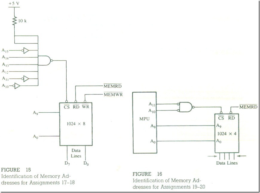
17. Identify the memory address range in Figure 15. List the high-order and low-order address lines. How many pages of memory does the chip include?
18. In Figure 2.IS, identify the address range if the inverter of the address line AIS is eliminated and AIS is connected directly to the NAND gate.
19. Figure 2.16 shows an MPU with the address bus containing 12 address lines and the data bus with four data lines; it is interfaced with the 1024 x 4 memory chip. Find the memory address range.
20. Specify the size of the memory word shown in Figure 16.
FIGURE 15 Identification of Memory Addresses for Assignments 17-18 FIGURE 16 Identification of Memory Addresses for Assignments 19-20
Labels: MPU memory I/O