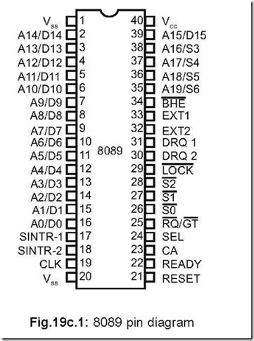
1. Draw the pin connection diagram of 8089.
Ans. The pin connection diagram of 8089 is shown in Fig. 19c.1.
2. Draw the functional block diagram of 8089.
Ans. The functional block diagram of 8089 is shown in Fig. 19c.2.
3. Write down the characteristic features of 8089. Ans. The characteristic features of 8089 are as follows:
z Very high speed DMA capability—I/O to memory, memory to I/O, memory to
memory and I/O to I/O.
z 1 MB address capability.
z iAPX 86, 88 compatible.
z Supports local mode and remote mode I/O processing.
z Allows mixed interface of 8-and 16-bit peripherals, to 8-and 16-bit processor buses.
z Multibus compatible system interface.
z Memory based communications with CPU.
z Flexible, intelligent DMA functions, including translation, search, word assembly/
disassembly.
z Supports two I/O channels.
4. Indicate the data transfer rate of 8089 IOP.
Ans. On each of the two channels of 8089, data can be transferred at a maximum rate of 1.25 MB/second for 5MHz clock frequency.
5. Mention a few application areas of 8089. Ans. A few of the application areas of 8089 are:
z File and buffer management in hard disk/floppy disk control.
z Provides for soft error recovery routines and scan control.
z CRT control such as cursor control and auto scrolling made simple with 8089.
z Keyboard control, communication control, etc.
6. Compare 8089 IOP with 8255 PPI and 8251 USART.
Ans. 8089 IOP is a front-end processor for the 8086/88 and 80186/88. In a way, 8089 is a microprocessor designed specifically for I/O operations. 8089 is capable of concurrent
operation with the host CPU when 8089 executes a program task from its own private memory.
8255 PPI and 8251 USART are peripheral controller chips designed to simplify I/O hardware design by incorporating all the logic for parallel (in case of 8255) or serial (in case of 8251) ports in one single package. These two chips need to be initialized for them to be used. But data transfer is controlled by CPU.
8089 IOP does not have any built-in I/O ports, not it is a replacement for 8255 or 8251. For I/O operations, 8089 executes the I/O related softwares, previously run by CPU (when no 8089 was used).
Thus in situations where I/O related operations are in a majority, 8089 does all these jobs independent of CPU. Once done, the host CPU communicates with 8089 for high speed data transfer either way.
7. Does 8089 generate any control signals.
Ans. No, 8089 does not output control bus signals: IOW, IOR, MEMR, MEMW, DT/ R, ALE and DEN. These signals are encoded into S0 − S2 signals, which are output pins for 8089 and are connected to the corresponding pins of 8288 bus controller and 8289
bus arbiter to generate memory and I/O control signals. The bus controller then outputs
all the above stated control bus signals. The S0 − S2 signals are encoded as follows
These signals change during T4 if a new cycle is to be entered. The return to passive state in T3 or TW indicates the end of a cycle. These pins float after a system reset— when the bus is not required.
8. Explain the utility of LOCK signal.
Ans. It is an output signal and is set via the channel control register and during the TSL instruction. This pin floats after a system reset—when the bus is not required.
The LOCK signal is meant for the 8289 bus arbiter and when active, this output pin prevents other processors from accessing the system buses. This is done to ensure that the system memory is not allowed to change until the locked instructions are executed.
9. Explain DRQ1-2 and EXT1-2 pins.
Ans. DRQ and EXT stand for Data Request and External Terminate, both being input pins— DRQ1 and EXT1 for channel 1 and DRQ2 and EXT2 for channel 2.
DRQ is used to initiate DMA transfer while EXT for termination of the same. A high on DRQ1 tells 8089 that a peripheral is ready to receive/transfer data via channel 1. DRQ must be held active (= 1) until the appropriate fetch/stroke is initiated.
A high on EXT causes termination of current DMA operation if the channel is so programmed by the channel control register. This signal must be held active (= 1) until termination is complete.
10. Explain the common control unit (CCU) block.
Ans. 8089 IOP has two channels. The activities of these two channels are controlled by CCU. CCU determines which channel—1 or 2 will execute the next cycle. In a particular case where both the channels have equal priority, an interleave procedure is adopted in which each alternate cycle is assigned to channels 1 and 2.
11. Explain the purpose of assembly/disassembly registers.
Ans. This permits 8089 to deal with 8-or 16-bit data width devices or a mix of both. In a particular case of an 8–bit width I/O device inputting data to a 16-bit memory interface, 8089 capture two bytes from the device and then write it into the assigned memory locations—all with the help of assembly/disassembly register.
12. Explain SINTR pin.
Ans. SINTR stands for signal interrupt. It is an output pin from 8089 and there are two such output pin SINTR1 and SINTR2—for channel 1 and 2 respectively.
Like 8087, 8086 does not communicate with 8089 directly. Normally, this takes place via a series of commonly accessible message blocks in system memory.
SINTR pin is another method of such communication. This output pin of 8087 can
be connected directly to the host CPU (8086) or through an 8259 interrupt controller. A high on this pin alerts the CPU that either the task program has been completed or else an error condition has occurred.
13. Elaborate on the communication between CPU and IOP with the help of communication data structure hierarchy.
Ans. Communication between the CPU and IOP takes place through messages in shared memory and consists of five linked memory message blocks (ABCDE or ABCD′E′ ) with ABC representing the initialisation process. The process of initialisation begins with 8089 IOP receiving a reset at its RESET input. The following occurs in sequence:
z On the falling edge of CA, the SEL input is sensed. SEL = 0/1 represent Master (Remote)/Slave (Local) configuration. (To note: during any other CA, the SEL line indicates selection of CH1/CH2 depending on SEL = 0/1 respectively).
z 5 bytes of information from system memory starting from FFFF6 H is read into 8089.
The first byte determines the width of the system bus. The subsequent bytes are then read to get the system configuration pointer (SCP) which gives the locations of the system configuration block (SCB).
![]()
![]() z The first byte existing at the base of SCB is read off, which determines the width of the 8089’s Private Bus and the operating mode of RQ / GT is defined. The base (or starting) address of control block (CB) is then read.
z The first byte existing at the base of SCB is read off, which determines the width of the 8089’s Private Bus and the operating mode of RQ / GT is defined. The base (or starting) address of control block (CB) is then read.
z The BUSY flag in CB is removed, signalling the end of the initialisation process.
It should be noted that the address of SCP—the system configuration pointer resides
in ROM and is the only one to have fixed address in the hierarchy. Since SCB resides
in RAM, hence it can be changed to accommodate additional IOPs, to be inducted into
the system.
All except the task block must be located in memory accessible to the 8089 and the host processor.
Once initialisation is over, any subsequent hardware CA input to IOP accesses the control block (CB) bytes for a particular channel—the channel (1 or 2) which gets selected depends on the SEL status. First the CCW (Channel Control Word) is read. Next the base address for the parameter block (PB) is read. This is also called data memory. Except the first two words, this PB block is user defined and is used to pass appropriate parameters to IOP for task block (TB), also called program memory. The task block can be terminated/restarted by the CPU.
This hierarchical data structure between the CPU and IOP gives modularity to system design and also future compatibility to future end users.
14. Show the channel register set model and discuss. Ans. The channel register set for 8089 IOP is shown in Fig.19c.4.
Registers GA, GB and GC and TP may address 1 MB of memory space (with tag bit = 0) or 64 KB of I/O space (with tag bit = 1). These four registers as also PP are called pointer registers.
The rest four registers—IX, BC, MC and CC are all 16 bits wide. Several DMA options can be programmed with the help of register CC.
15. Mention the addressing modes of 8089 IOP.
Ans. 8089 IOP has six different addressing modes. These are:
z Register addressing
z Immediate addressing
z Offset addressing
z Based addressing
z Indexed addressing and
z Indexed with auto increment addressing.
Labels: Microprocessors And Peripheral ICs Questions And Answers