Basic blocks of a microcomputer , typical microcomputer architecture and the single-chip microprocessor
6.1 Basic Blocks of a Microcomputer
A microcomputer has three basic blocks: a central processing unit (CPU), a memory unit, and an input/output unit. The CPU executes all the instructions and performs arithmetic and logic operations on data. The CPU of the microcomputer is called the "microprocessor." The microprocessor is typically a single VLSI (Very Large-Scale Integration) chip that contains all the registers, control unit, and arithmetic/ logic circuits of the microcomputer.
A memory unit stores both data and instructions. The memory section typically
contains ROM and RAM chips. The ROM can only be read and is nonvolatile, that is, it retains its contents when the power is turned off. A ROM is typically used to store instructions and data that do not change. For example, it might store a table of codes for outputting data to a display external to the microcomputer for turning on a digit from 0 to 9.
One can read from and write into a RAM. The RAM is volatile; that is, it does
not retain its contents when the power is turned off. A RAM is used to store programs and data that are temporary and might change during the course of executing a program. An I/0 (Input/Output) unit transfers data between the microcomputer and the external devices via I/0 ports (registers). The transfer involves data, status, and control signals.
In a single-chip microcomputer, these three elements are on one chip, whereas with a single-chip microprocessor, separate chips for memory and 1/0 are required. Microcontrollers evolved from single-chip microcomputers. The microcontrollers are typically used for dedicated applications such as automotive systems, home appliances, and home entertainment systems. Typical microcontrollers, therefore, include on-chip timers and AID (analog to digital) and D/A (digital to analog) converters. Two popular

microcontrollers are the Intel 8751 (8 bit)/8096 ( 16 bit) and the Motorola HC 11 (8 bit)/ HC16 (16 bit). The 16-bit microcontrollers include more on-chip ROM, RAM, and I/0 than the 8-bit microcontrollers. Figure 6.1 shows the basic blocks of a microcomputer. The System bus (comprised of several wires) connects these blocks.
6.2 Typical Microcomputer Architecture
In this section, we describe the microcomputer architecture in more detail. The various microcomputers available today are basically the same in principle. The main variations are in the number of data and address bits and in the types of control signals they use.
To understand the basic principles of microcomputer architecture, it is necessary to investigate a typical microcomputer in detail. Once such a clear understanding is obtained, it will be easier to work with any specific microcomputer. Figure 6.2 illustrates the most simplified version of a typical microcomputer. The figure shows the basic blocks of a microcomputer system. The various buses that connect these blocks are also shown. Although this figure looks very simple, it includes all the main elements of a typical microcomputer system.
6.2.1 The Microcomputer Bus
The microcomputer's system bus contains three buses, which carry all the address, data, and control information involved in program execution. These buses connect the microprocessor (CPU) to each of the ROM, RAM, and I/O chips so that information transfer between the microprocessor and any of the other elements can take place.
In the microcomputer, typical information transfers are carried out with respect to the memory or I/0. When a memory or an I/O chip receives data from the microprocessor
, it is called a WRITE operation, and data is written into a selected memory location or an I/O port (register). When a memory or an I/O chip sends data to the microprocessor,
it is called a READ operation, and data is read from a selected memory location or an I/O port.
In the address bus, information transfer takes place only in one direction, from the microprocessor to the memory or I/O elements. Therefore, this is called a "unidirectional bus." This bus is typically 20 to 32 bits long. The size of the address bus determines the total number of memory addresses available in which programs can be executed by the microprocessor. The address bus is specified by the total number of address pins on the microprocessor chip. This also determines the direct addressing capability or the size of the main memory of the microprocessor. The microprocessor can only execute the programs located in the main memory. For example, a microprocessor with 20 address pins can generate 220 = 1,048,576 (one megabyte) different possible addresses (combinations of 1's and O's) on the address bus. The microprocessor includes addresses from 0 to 1,048,575 (0000016 through FFFFF16). A memory location can be represented by each one of these
addresses. For example, an 8-bit data item can be stored at address 00200 16•
When a microprocessor such as the 8086 wants to transfer information between itself and a certain memory location, it generates the 20-bit address from an internal register on its 20 address pins A0-A 19, which then appears on the address bus. These 20 address bits are decoded to determine the desired memory location. The decoding process normally requires hardware (decoders) not shown in Figure 6.2.
In the data bus, data can flow in both directions, that is, to or from the
microprocessor. Therefore, this is a bidirectional bus. In some microprocessors, the data pins are used to send other information such as address bits in addition to data. This means that the data pins are time-shared or multiplexed. The Intel 8086 microprocessor is an example where the 20 bits of the address are multiplexed with the 16-bit data bus and four status lines.
The control bus consists of a number of signals that are used to synchronize the
operation of the individual microcomputer elements. The microprocessor sends some of these control signals to the other elements to indicate the type of operation being performed. Each microcomputer has a unique set of control signals. However, there are some control signals that are common to most microprocessors. We describe some of these control signals later in this section.
6.2.2 Clock Signals
The system clock signals are contained in the control bus. These signals generate the appropriate clock periods during which instruction executions are carried out by the microprocessor. The clock signals vary from one microprocessor to another. Some microprocessors have an internal clock generator circuit to generate a clock signal. These microprocessors require an external crystal or an RC network to be connected at the appropriate microprocessor pins for setting the operating frequency. For example, the Intel 80186 (16-bit microprocessor) does not require an external clock generator circuit. However, most microprocessors do not have the internal clock generator circuit and require an external chip or circuit to generate the clock signal. Figure 6.3 shows a typical clock signal.


6.3 The Single-Chip Microprocessor
As mentioned before, the microprocessor is the CPU of the microcomputer. Therefore, the power of the microcomputer is determined by the capabilities of the microprocessor. Its clock frequency determines the speed of the microcomputer. The number of data and address pins on the microprocessor chip make up the microcomputer's word size and maximum memory size. The microcomputer's I/O and interfacing capabilities are determined by the control pins on the microprocessor chip.
The logic inside the microprocessor chip can be divided into three main areas: the
register section, the control unit, and the arithmetic and logic unit (ALU). A microprocessor chip with these three sections is shown in Figure 6.4. We now describe these sections.
6.3.1 Register Section
The number, size, and types of registers vary from one microprocessor to another. However, the various registers in all microprocessors carry out similar operations. The register structures of microprocessors play a major role in designing the microprocessor architectures. Also, the register structures for a specific microprocessor determine how convenient and easy it is to program this microprocessor.
We first describe the most basic types of microprocessor registers, their functions,
and how they are used. We then consider the other common types of registers.
Basic Microprocessor Registers
There are four basic microprocessor registers: instruction register, program counter, memory address register, and accumulator.
• Instruction Register (IR). The instruction register stores instructions. The contents of an instruction register are always decoded by the microprocessor as an instruction. After fetching an instruction code from memory, the microprocessor stores it in the instruction register. The instruction is decoded internally by the microprocessor, which then performs the required operation. The word size of the microprocessor determines the size of the instruction register. For example, a 16-bit microprocessor has a 16-bit instruction register.
Program Counter (PC). The program counter contains the address of the instruction
or operation code (op-code). The program counter normally contains the address of the next instruction to be executed. Note the following features of the program counter:
1. Upon activating the microprocessor's RESET input, the address of the first
instruction to be executed is loaded into the program counter.
2. To execute an instruction, the microprocessor typically places the contents of the program counter on the address bus and reads ("fetches") the contents of this address, that is, instruction, from memory. The program counter contents are automatically incremented by the microprocessor's internal logic. The microprocessor thus executes a program sequentially, unless the program contains an instruction such as a JUMP instruction, which changes the sequence.
3. The size of the program counter is determined by the size of the address bus.
4. Many instructions, such as JUMP and conditional JUMP, change the contents of the program counter from its normal sequential address value. The program counter is loaded with the address specified in these instructions.
Memory Address Register (MAR). The memory address register contains the
address of data. The microprocessor uses the address, which is stored in the memory address register, as a direct pointer to memory. The contents of the address consists of the actual data that is being transferred.
Accumulator (A). For an 8-bit microprocessor, the accumulator is typically an 8-bit
register. It is used to store the result after most ALU operations. These microprocessors have instructions to shift or rotate the accumulator 1 bit to the right or left through the carry flag. The accumulator is typically used for inputting a byte into the accumulator from an external device or outputting a byte to an external device from the accumulator. Some microprocessors, such as the Motorola 6809, have more than one accumulator. In these microprocessors, the accumulator to be used by the instruction is specified in the op-code.
Depending on the register section, the microprocessor can be classified either as an accumulator-based or a general-purpose register-based machine. In an accumulator-based microprocessor such as the Intel 8085 and Motorola 6809, the data is assumed to be held in a register called the "accumulator." All arithmetic and logic operations are performed using this register as one of the data sources. The result after the operation is stored in the accumulator. Eight-bit microprocessors are usually accumulator based.
The general-purpose register-based microprocessor is usually popular with 16- , 32-, and 64-bit microprocessors, such as the Intel 8086/80386/80486/Pentium and the Motorola 68000/68020 /68030 /68040 /PowerPC. The term "general-purpose" comes from the fact that these registers can hold data, memory addresses, or the results of arithmetic or logic operations. The number, size, and types of registers vary from one microprocessor to another.
Most registers are general-purpose whereas some, such as the program counter
(PC), are provided for dedicated functions. The PC normally contains the address of the next instruction to be executed. As metioned before, upon activating the microprocessor chi p's RESET input pin, the PC is normally initialized with the address of the first instruction. For example, the 80486, upon hardware reset, reads the first instruction from the 32-bit hex address FFFFFFF0. To execute the instruction, the microprocessor normally places the PC contents on the address bus and reads (fetches) the first instruction from external memory. The program counter contents are then automatically incremented by the ALU. The microcomputer thus usually executes a program sequentially unless it encounters a jump or branch instruction. As mentioned earlier, the size of the PC varies from one microprocessor to another depending on the address size. For example, the 68000 has a 24-bit PC, whereas the 68040 contains a 32-bit PC. Note that in general-purpose register based microprocessors, the four basic registers typically include a PC, an MAR, an IR, and a data register.
Use of the Basic Microprocessor Registers
To provide a clear understanding of how the basic microprocessor registers are used, a binary addition program will be considered. The program logic will be explained by showing how each instruction changes the contents of the four registers. Assume that all numbers are in hex. Suppose that the contents of the memory location 2010 are to be added with the contents of 2012. Assume that [NNNN] represents the contents of the memory
location NNNN. Now, suppose that [2010] = 0002 and [2012] = 0005. The steps involved in accomplishing this addition can be summarized as follows:
1. Load the memory address register (MAR) with the address of the first data item to be added, that is, load 2010 into MAR.
2. Move the contents of this address to a data register, D0; that is, move first data into D0.
3. Increment the MAR by 2 to hold 2012, the address of the second data item to be added.
4. Add the contents of this memory location to the data that was moved to the data register, D0 in step 2, and store the result in the 16-bit data register, D0. The above addition program will be written using 68000 instructions. Note that the 68000 uses 24-bit addresses; 24-bit addresses such as 002000 16 will be represented as 2000 16 (16-bit number) in the following.
The following steps will be used to achieve this addition for the 68000:
1. Load the contents of the next 16-bit memory word into the memory address register, AI. Note that register A1 can be considered as MAR in the 68000.
2. Read the 16-bit contents of the memory location addressed by MAR into data register, DO.
3. Increment MAR by 2 to hold 2012, the address of the second data to be added.
4. Add the current contents of data register, D0 to the contents of the memory location whose address is in MAR and store the 16-bit result in D0.
The following steps for the Motorola 68000 will be used to achieve the above addition:

The complete program in hexadecimal, starting at location 2000 16 (arbitrarily chosen) is given in Figure 6.5. Note that each memory address stores 16bits. Hence, memory addresses are shown in increments of 2. Assume that the microcomputer can be instructed that the starting address of the program is 2000 16• This means that the program counter can be initialized to contain 2000 16, the address of the first instruction to be executed. Note that the contents of the other three registers are not known at this point. The microprocessor loads the contents of memory location addressed by the program counter into IR. Thus, the first instruction, 3279 16,stored in address 2000 16 is transferred into IR.
The program counter contents are then incremented by 2 by the microprocessor's
ALU to hold 2002 16• The register contents that result along with the program are shown in Figure 6.6.
The binary code 3279 16 in the IR is executed by the microprocessor. The microprocessor then takes appropriate actions. Note that the instruction, 3279 16, loads the contents of the next memory location addressed by the PC into the MAR. Thus, 2010 16 is loaded into the MAR. The contents of the PC are then incremented by 2 to hold 2004 16• This is shown in Figure 6.7.


Next, the microprocessor loads the contents of the memory location addressed by the PC into theIR; thus, 30 I 016 is loaded into theIR. The PC contents are then incremented by 2 to hold 2006 16• This is shown in Figure 6.8. In response to the instruction 301016, the contents of the memory location addressed by the MAR are loaded into the data register, D0; thus, 0002 16 is moved to register D0. The contents of the PC are not incremented this time. This is because 0002 16 is not immediate data. Figure 6.9 shows the details. Next the microprocessor loads 524916 to IR and then increments PC to contain 2008 16 as shown in Figure 6.10.
In response to the instruction 524916 in the IR, the microprocessor increments the MAR by 2 to contain 2012 16 as shown in Figure 6.11. Next, the instruction D051 16 in location 2008 16 is loaded into theIR, and the PC is then incremented by 2 to hold 200A 16 as shown in Figure 6.12. Finally, in response to instruction D051 16, the microprocessor adds the contents of the memory location addressed by MAR (address 2012 16) with the contents of register D0 and stores the result in D0. Thus, 0002 16 is added with 0005 16,and the 16-bit result 0007 16 is stored in D0 as shown in Figure 6.13. This completes the execution of the binary addition program.

• General-Purpose Registers
The 16-, 32-, and 64-bit microprocessors are register oriented. They have a number of general-purpose registers for storing temporary data or for carrying out data transfers between various registers. The use of general-purpose registers speeds up the execution of a program because the microprocessor does not have to read data from external memory via the data bus if data is stored in one of its general-purpose registers. These registers are typically 16 to 32 bits. The number of general-purpose registers will vary from one microprocessor to another. Some of the typical functions performed by instructions associated with the general-purpose registers are given here. We will use [REG] to indicate the contents of the general-purpose register and [M] to indicate the contents of a memory location.


• Index Register
An index register is typically used as a counter in address modification for an instruction, or for general storage functions. The index register is particularly useful with instructions that access tables or arrays of data. In this operation the index register is used to modify the address portion of the instruction. Thus, the appropriate data in a table can be accessed. This is called "indexed addressing." This addressing mode is normally available to the programmers of microprocessors. The effective address for an instruction using the indexed addressing mode is determined by adding the address portion of the instruction to the contents of the index register. Index registers are typically 16 or 32 bits long. In a typical 16- or 32-bit microprocessor, general purpose registers can be used as index registers.
• Status Register
The status register, also known as the "processor status word register" or the "condition code register," contains individual bits, with each bit having special significance. The bits in the status register are called "flags." The status of a specific microprocessor operation is indicated by each flag, which is set or reset by the microprocessor's internal logic to indicate the status of certain microprocessor operations such as arithmetic and
logic operations. The status flags are also used in conditional JUMP instructions. We will describe some of the common flags in the following.
The carryflag is used to reflect whether or not the result generated by an arithmetic operation is greater than the microprocessor's word size. As an example, the addition of two 8-bit numbers might produce a carry. This carry is generated out of the eighth position, which results in setting the carry flag. However, the carry flag will be zero if no carry is generated from the addition. As mentioned before, in multibyte arithmetic, any carry out of the low-byte addition must be added to the high-byte addition to obtain the correct result. This can illustrated by the following example:

While performing BCD arithmetic with microprocessors, the carry out of the low nibble (4 bits) has a special significance. Because a BCD digit is represented by 4 bits, any carry out of the low 4 bits must be propagated into the high 4 bits for BCD arithmetic. This carry flag is known as the auxiliary carry flag and is set to I if the carry out of the low 4 bits is 1, otherwise it is 0.
A zero flag is used to show whether the result of an operation is zero. It is set to 1 if the result is zero, and it is reset to 0 if the result is nonzero. A parity flag is set to I to indicate whether the result of the last operation contains either an even number of I 's (even parity) or an odd number of I 's (odd parity), depending on the microprocessor. The type of parity flag used (even or odd) is determined by the microprocessor's internal structure and is not selectable. The sign flag (also sometimes called the negative flag) is used to indicate whether the result of the last operation is positive or negative. If the most significant bit of the last operation is I, then this flag is set to I to indicate that the result is negative. This flag is reset to 0 if the most significant bit of the result is zero, that is, if the result is positive.
As mentioned before, the overflow flag arises from the representation of the sign flag by the most significant bit of a word in signed binary operation. The overflow flag is set to I if the result of an arithmetic operation is too big for the microprocessor's maximum word size, otherwise it is reset to 0. Let C1be the final carry out of the most significant bit (sign bit) and CP be the previous carry. It was shown in Chapter 2 that the overflow flag is the exclusive OR of the carries CP and Cp
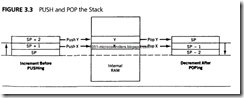
• Stack Pointer Register
The stack consists of a number of RAM locations set aside for reading data from or writing data into these locations and is typically used by subroutines (a subroutine is a program that performs operations frequently needed by the main or calling program). The address of the stack is contained in a register called the "stack pointer." Two instructions, PUSH and POP, are usually available with the stack. The PUSH operation
![image_thumb[1]](https://blogger.googleusercontent.com/img/b/R29vZ2xl/AVvXsEjZOGPnXPxGr0wXzrt8sKH06_qSaNa5FCpRre7AnvTMubT5mJU-KJwZjTI5yCXZtNEYR9jQWlBxRkUguCOK3fZ3RWH5snPGXyZbfuqJGgnrHMtG0rhyphenhyphenmRNQEw2B5T6A9GwHAdqwhhsx/s1600-h/image_thumb%25255B1%25255D%25255B3%25255D.png "image_thumb[1]")
![image_thumb[2]](https://blogger.googleusercontent.com/img/b/R29vZ2xl/AVvXsEjM8ZkuPUW3ZUkK6oy5u_3b8qltLLFTe8g6PcaOnHvy2VimslUtOLMJd8QGCKK9HYgPIX7ygBnNI1a5VFW59oxM4jXPVRJE-pM-zpy6CrI39EXGPU0VlwUzPTqEl8yEOW_sMuOl81yO/s1600-h/image_thumb%25255B2%25255D%25255B3%25255D.png "image_thumb[2]")
![image_thumb[3]](https://blogger.googleusercontent.com/img/b/R29vZ2xl/AVvXsEhPjANmbnWZMbqFS1goOJXSA1TzmUeElKa-8Q6mUGeQPfEugBdT2-ZeW5wtsKVmM3HblYgv7t6Da4w-lHp1WV0r8Zadl2nQtw6CyZCDFLW9uUpsjmG9TqKcc187Bnc6XxOuGOyYDDVf/s1600-h/image_thumb%25255B3%25255D%25255B3%25255D.png "image_thumb[3]")
is defined as writing to the top or bottom of the stack, whereas the POP operation means reading from the top or bottom of the stack. Some microprocessors access the stack from the top; the others access via the bottom. When the stack is accessed from the bottom, the stack pointer is incremented after a PUSH and decremented after a POP operation. On the other hand, when the stack is accessed from the top, the stack pointer is decremented after a PUSH and incremented after a POP. Microprocessors typically use 16- or 32-bit registers for performing the PUSH or POP operations. The incrementing or decrementing of the stack pointer depends on whether the operation is PUSH or POP and also whether the stack is accessed from the top or the bottom.
We now illustrate the stack operations in more detail. We use 16-bit registers in
Figures 6.14 and 6.15. In Figure 6.14, the stack pointer is incremented by 2 (since 16- bit register) to address location 20C7 after the PUSH. Now consider the POP operation of Figure 6.15. Note that after the POP, the stack pointer is decremented by 2. [20C5] and [20C6) m:e assumed to be empty conceptually after the POP operation. Finally, consider the PUSH operation of Figure 6.16. The stack is accessed from the top. Note that'the stack pointer is decremented by 2 after a PUSH. Next, consider the POP (Figure 6.17). [20C4] and [20C5) are assumed to be empty after the POP.
Note that the stack is a LIFO (Last In First Out) memory.
Example 6.1
Determine the carry (C), sign (S), zero (Z), overflow (V), and parity (P) flags for the following operation: 01102 plus 10102 •
Assume the parity bit = 1 for ODD parity in the result; otherwise the parity bit = 0. Also, assume that the numbers are signed. Draw a logic diagram for implementing the flags in a 5-bit register using D flip-flops; use P = bit 0, V = bit 1, Z =bit 2, S = bit 3, and C =bit 4. Note that Verilog and VHDL descriptions along with simulation results of this status register are provided in Appendices I and J respectively.
![image_thumb[4]](https://blogger.googleusercontent.com/img/b/R29vZ2xl/AVvXsEjrWJILJuhYKAfXkYBTF85m-2nsYP3eCB-AyfChqbhFzFv-ZG8wAm-GrVz7P3pTjCh2D0VGvmcDGBm9F5UBi4XfepVSQsIZvmpcSBeRuNkNUuXNHTSikxzgZeZBkQbdaar1qxPEj5kg/s1600-h/image_thumb%25255B4%25255D%25255B3%25255D.png "image_thumb[4]")
The flag register can be implemented from the 4-bit result as follows:
![image_thumb[5]](https://blogger.googleusercontent.com/img/b/R29vZ2xl/AVvXsEiSpmwsSUxj1e-zIZ3R_TmqpYRAol4Xmwb1EpHyGCQw1pgzQ1N4X6WV2h_ZOgpVETbe-lAc_fXBzH2LdwuzFrYpTILCdhuwM-S7h8xVd1mFPvRZQJHCGfMKOs0c-kXyEH8qx8IOpMvf/s1600-h/image_thumb%25255B5%25255D%25255B3%25255D.png "image_thumb[5]")
6.3.2 Control Unit
The main purpose of the control unit is to read and decode instructions from the program memory. To execute an instruction, the control unit steps through the appropriate blocks of the ALU based on the op-codes contained in the instruction register. The op-codes define the operations to be performed by the control unit in order to execute an instruction. The control unit interprets the contents of the instruction register and then responds to the instruction by generating a sequence of enable signals. These signals activate the appropriate ALU logic blocks to perform the required operation.
The control unit generates the control signals, which are output to the other microcomputer elements via the control bus. The control unit also takes appropriate actions in response to the control signals on the control bus provided by the other microcomputer elements.
The control signals vary from one microprocessor to another. For each specific microprocessor, these signals are described in detail in the manufacturer's manual. It is impossible to describe all the control signals for various manufacturers. However, we cover some of the common ones in the following discussion.
- RESET. This input is common to all microprocessors. When this input pin is driven to HIGH or LOW (depending on the microprocessor), the program counter is loaded with a predefined address specified by the manufacturer. For example, in the 80486, upon hardware reset, the program counter is loaded with FFFFFFF0 16• This means that the instruction stored at memory location FFFFFFF0 16 is executed first. In some other microprocessors, such as the Motorola 68000, the program counter is not loaded directly by activating the RESET input. In this case, the program counter is loaded indirectly from two locations (such as 000004 and 000006) predefined by the manufacturer. This means that these two locations contain the address of the first instruction to be executed.
- READ/WRITE (RIW). This output line is common to all microprocessors. The status of this line tells the other microcomputer elements whether the microprocessor is performing a READ or a WRITE operation. A HIGH signal on this line indicates a READ operation and a LOW indicates a WRITE operation. Some microprocessors have separate READ and WRITE pins.
- READY. This is an input to the microprocessor. Slow devices (memory and I/0) use this signal to gain extra time to transfer data to or receive data from a microprocessor. The READY signal is usually an active low signal, that is, LOW means that the microprocessor is ready. Therefore, when the microprocessor selects a slow device, the device places a LOW on the READY pin. The microprocessor responds by suspending all its internal operations and enters a WAIT state. When the device is ready to send or receive data, it removes the READY signal. The microprocessor comes out of the WAIT state and performs the appropriate operation.
- Interrupt Request (INT or IRQ). The external I/0 devices can interrupt the microprocessor via this input pin on the microprocessor chip. When this signal is activated by the external devices, the microprocessor jumps to a special program, called the "interrupt service routine." This program is normally written by the user for performing tasks that the interrupting device wants the microprocessor to do. After completing this program, the microprocessor returns to the main program it was executing when the interrupt occurred.
6.3.3 Arithmetic and Logic Unit (ALU)
The ALU performs all the data manipulations, such as arithmetic and logic operations, inside the microprocessor. The size of the ALU conforms to the word length of the microcomputer. This means that a 32-bit microprocessor will have a 32-bit ALU. Typically, the ALU performs the following functions:
I. Binary addition and logic operations
2. Finding the ones complement of data
3. Shifting or rotating the contents of a general-purpose register I bit to the left or right through carry
6.3.4 Functional Representations of a Simple and a Typical Microprocessor
Figure 6.18 shows the functional block diagram of a simple microprocessor. Note that the
![image_thumb[6]](https://blogger.googleusercontent.com/img/b/R29vZ2xl/AVvXsEhIWQO9EoyvLeaQG-vijwfAtIESXzX9dD90XB01oEgDINoF8hQXEWRgWWTvgV9Mgyh8x8r5WEjrIBVWKsCLb796lgalhHK4ZwgC9OPdxtzbH94Te3Ko2o36EaSA5jYdGHhLI92_6bYa/s1600-h/image_thumb%25255B6%25255D%25255B3%25255D.png "image_thumb[6]")
![image_thumb[7]](https://blogger.googleusercontent.com/img/b/R29vZ2xl/AVvXsEhKsk1VmR5Rp1rCCH4bL8LXjhwgbwpVNhssS3kWbRxsaM6I-9VA98c3MrbS24pgeNNPtGMMDclP2BR65O0nfAwuFIUYlh7obSe6eHDPM2iX8ZIdemuN6NunuxdEKfLujj5asgXBiFZE/s1600-h/image_thumb%25255B7%25255D%25255B3%25255D.png "image_thumb[7]")
data bus shown is internal to the microprocessor chip and should not be confused with the system bus. The system bus is external to the microprocessor and is used to connect all the necessary chips to form a microcomputer. The buffer register in Figure 6.18 stores any data read from memory for further processing by the ALU. All other blocks of Figure 6.18 have been discussed earlier. Figure 6.19 shows the simplified block diagram of a realistic microprocessor, the Intel 8086.
The 8086 microprocessor is internally divided into two functional units: the bus interface unit (BIU) and the execution unit (EU). The BIU interfaces the 8086 to external memory and 110 chips. The BIU and EU function independently. The BIU reads (fetches) instructions and writes or reads data to or from memory and 110 ports. The EU executes instructions that have already been fetched by the BIU. The BIU contains segment registers, the instruction pointer (IP), the instruction queue registers, and the address generation/bus control circuitry.
The 8086 uses segmented memory. This means that the 8086 's 1 MB main memory is divided into 16 segments of 64 KB each. Within a particular segment, the instruction pointer (IP) works as a program counter (PC). Both the IP and the segment registers are 16 bits wide. The 20-bit address is generated in the BIU by using the contents of a 16-bit IP and a 16-bit segment register. The ALU in the BIU is used for this purpose. Memory segmentation is useful in a time-shared system when several users share a microprocessor. Segmentation makes it easy to switch from one user program to another by changing the
contents of a segment register.
The bus control logic of the BIU generates all the bus control signals such as read and write signals for memory and I/0. The BIU's instruction register consist of a first in-first-out (FIFO) memory in which up to six instruction bytes are preread (prefetched) from external memory ahead of time to speed up instruction execution. The control unit in the EU translates the instructions based on the contents of the instruction registers in the BIU.
The EU contains severall6-bit general-purpose registers. Some of them are AX, BX, CX, and DX. Each of these registers can be used either as an 8-bit register (AH, AL, BH, BL, CH, CL, DH, DL) or as a 16-bit register (AX, BX, CX, DX). Register BX can also be used to hold the address in a segment. The EU also contain a 16-bit status register. The ALU in the EU performs all arithmetic and logic operations. The 8086 is covered in detail in Chapter 9.
6.3.5 Microprogramming the Control Unit (A Simplified Explanation)
In this section, we discuss how the op-codes are interpreted by the microprocessor. Most microprocessors have an internal memory, called the "control memory" (ROM). This memory is used to store a number of codes, called the "microinstructions." These microinstructions are combined together to design instructions. Each instruction in the instruction register initiates execution of a set of microinstructions in the control unit to perform the operation required by the instruction. The microprocessor manufacturers define the microinstructions by programming the control memory (ROM) and thus, design the instruction set of the microprocessor. This type of programming is known as "microprogramming." Note that the control units of most 16-, 32-, and 64-bit microprocessors are microprogrammed.
For simplicity, we illustrate the concepts of microprogramming using Figure
6.18. Let us consider incrementing the contents of the register. This is basically an addition operation. The control unit will send an enable signal to execute the ALU adder logic.
![image_thumb[8]](https://blogger.googleusercontent.com/img/b/R29vZ2xl/AVvXsEiZBhULNyjhDwi97n_jb16mIdol4ETN8-k6_tv-P8_nT4dChbPhGVElDUvOSLoIDCk-2NOJjlcqzfpZEN5RGHKSRxMXfiPBa7PQkw4ueJdBfMAm8BgdGevuh_pgtTEEbOnjiBbmQclM/s1600-h/image_thumb%25255B8%25255D%25255B3%25255D.png "image_thumb[8]")
Incrementing the contents of a register consists of transferring the register contents to the ALU adder and then returning the result to the register. The complete incrementing process is accomplished via the five steps shown in Figures 6.20 through Figure 6.24. In all five steps, the control unit initiates execution of each microinstruction. Figure 6.20 shows the transfer of the register contents to the data bus. Figure 6.21 shows the transfer of the contents of the data bus to the adder in the ALU in order to add 1 to it. Figure 6.22 shows the activation of the adder logic. Figure 6.23 shows the transfer of the result from the adder to the data bus. Finally, Figure 6.24 shows the transfer of the data bus contents to the register.
Microprogramming is typically used by the microprocessor designer to program
the logic performed by the control unit. On the other hand, assembly language programming is a popular programming language used by the microprocessor user for programming the microprocessor to perform a desired function. A microprogram is stored in the control unit. An assembly language program is stored in the main memory. The assembly language program is called a macroprogram. A macroinstruction (or simply an instruction) initiates execution of a complete microprogram.
A simplified explanation of microprogramming is provided in this section. This topic will be covered in detail in Chapter 7.
![image_thumb[9]](https://blogger.googleusercontent.com/img/b/R29vZ2xl/AVvXsEgbXR_tTF3VVE0984IbQzLt4Id_b9zI355kJluyaw7kOHLf0DBQ0z7l-xJwTzZhvtXjXDRzvZl1FaDzOrnpmWi15NIzbNwfDhPLLp-3nUYWMN8sWkAMiftBrBkPzVeiZIwM06I4PVS8/s1600-h/image_thumb%25255B9%25255D%25255B3%25255D.png "image_thumb[9]")
![image_thumb[10]](https://blogger.googleusercontent.com/img/b/R29vZ2xl/AVvXsEiaO-g3YY2DkNng8eEWa4WGVED9JzePAGQpqApgYoa8QTx9AbpiOQindK3Fub_GP2IXCxVgP4URRMTzkeAGNaDBZBEi8e0um_i_KHg21VdL_w6EWTzcQNbN2c3jqTsKGv26znafXpbM/s1600-h/image_thumb%25255B10%25255D%25255B3%25255D.png "image_thumb[10]")
![image_thumb[11]](https://blogger.googleusercontent.com/img/b/R29vZ2xl/AVvXsEi9Q1LYzqSKZXctd1M8W3u9N_WBdb3525-_rB7ZrvLiXzJp32EI3BtwVKtlZbXCA-h7cr0XueJRvyxg5fkqgARi_Ekg7nhaeMGM3lc2f28XulrwFWnJq-Jz-pQvcPyF1qMCzxd6656s/s1600-h/image_thumb%25255B11%25255D%25255B3%25255D.png "image_thumb[11]")
![image_thumb[12]](https://blogger.googleusercontent.com/img/b/R29vZ2xl/AVvXsEhyk11MtemBJe60ApI6y3j11aeaKHPlKbBRBG3nFvLRaK76qQ9QQjdy6-Kpb5wldkag2vot0kzuEPSkA9HHKKU1xSgM-5QtU3-PRM5CXrTf5Jo-pv2uKa1Fp6XOWOOOFc16Hbuf3WMa/s1600-h/image_thumb%25255B12%25255D%25255B2%25255D.png "image_thumb[12]")

Comments
Post a Comment