THE 80186, 80188, AND 80286 MICROPROCESSORS:80186/80188 ARCHITECTURE.
THE 80186, 80188, AND 80286 MICROPROCESSORS
INTRODUCTION
The Intel 80186/80188 and the 80286 are enhanced versions of the earlier versions of the 80X86 family of microprocessors. The 80186/80188 and 80286 are all 16-bit microprocessors that are upward-compatible to the 8086/8088. Even the hardware of these microprocessors is similar to the earlier versions. This chapter presents an overview of each microprocessor and points out the differences or enhancements that are present in each version. The first part of the chapter describes the 80186/80188 microprocessors, and the last part shows the 80286 microprocessor.
New to recent editions is expanded coverage of the 80186/80188 family. Intel has added four new versions of each of these embedded controllers to its lineup of microprocessors. Each is a CMOS version and is designated with a two-letter suffix: XL, EA, EB, and EC. The 80C186XL and 80C188XL models are most similar to the earlier 80186/80188 models.
CHAPTER OBJECTIVES
Upon completion of this chapter, you will be able to:
1. Describe the hardware and software enhancements of the 80186/80188 and the 80286 microprocessors as compared to the 8086/8088.
2. Detail the differences between the various versions of the 80186 and 80188 embedded controllers.
3. Interface the 80186/80188 and the 80286 to memory and I/O.
4. Develop software using the enhancements provided in these microprocessors.
5. Describe the operation of the memory management unit (MMU) within the 80286 microprocessor.
6. Define and detail the operation of a real-time operating system (RTOS).
80186/80188 ARCHITECTURE
The 80186 and 80188, like the 8086 and 8088, are nearly identical. The only difference between the 80186 and 80188 is the width of their data buses. The 80186 (like the 8086) contains a 16-bit data bus, while the 80188 (like the 8088) contains an 8-bit data bus. The internal register structure of the 80186/80188 is virtually identical to that of the 8086/8088. About the only difference is that the 80186/80188 contain additional reserved interrupt vectors and some very powerful built-in I/O features. The 80186 and 80188 are often called embedded controllers because of their applica- tion as a controller, not as a microprocessor-based computer.
Versions of the 80186/80188
As mentioned, the 80186 and 80188 are available in four different versions, which are all CMOS microprocessors. Table 16–1 lists each version and the major features provided. The 80C186XL and 80C188XL are the most basic versions of the 80186/80188; the 80C186EC and 80C188EC are the most advanced. This text details the 80C186XL/80C188XL, and then describes the addi- tional features and enhancements provided in the other versions.
80186 Basic Block Diagram
Figure 16–1 provides the block diagram of the 80188 microprocessor that generically represents all versions except for the enhancements and additional features outlined in Table 16–1. Notice that this microprocessor has a great deal more internal circuitry than the 8088. The block diagrams of the 80186 and 80188 are identical except for the prefetch queue, which is four bytes in the 80188 and six bytes in the 80186. Like the 8088, the 80188 contains a bus interface unit (BIU) and an execution unit (ED).
In addition to the BIU and ED, the 80186/80188 family contains a clock generator, a pro- grammable interrupt controller, programmable timers, a programmable DMA controller, and a programmable chip selection unit. These enhancements greatly increase the utility of the 80186/80188 and reduce the number of peripheral components required to implement a system. Many popular subsystems for the personal computer use the 80186/80188 microprocessors as


caching disk controllers, local area network (LAN) controllers, and so forth. The 80186/80188 also finds application in the cellular telephone network as a switcher.
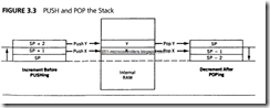
Software for the 80186/80188 is identical to that for the 80286 microprocessor, without the memory management instructions. This means that the 80286-like instructions for immediate multiplication, immediate shift counts, string I/O, PUSHA, POPA, BOUND, ENTER, and LEAVE all function on the 80186/80188 microprocessors.
80186/80188 Basic Features
In this segment of the text, we introduce the enhancements of the 80186/80188 microprocessors or embedded controllers that apply to all versions except where noted, but we do not provide exclusive coverage. More details on the operation of each enhancement and details of each advanced version are provided later in the chapter.
Clock Generator. The internal clock generator replaces the external 8284A clock generator used with the 8086/8088 microprocessors. This reduces the component count in a system.
The internal clock generator has three pin connections: X1, X2, and CLKOUT (or on some versions: CLKIN, OSCOUT, and CLKOUT). The X1 (CLKIN) and X2 (OSCOUT) pins are connected to a crystal that resonates at twice the operating frequency of the microprocessor. In the 8 MHz version of the 80186/80188, a 16 MHz crystal is attached to X1 (CLKIN) and X2 (OSCOUT). The 80186/80188 is available in 6 MHz, 8 MHz, 12 MHz, 16 MHz, or 25 MHz versions.
The CLKOUT pin provides a system clock signal that is one half the crystal frequency, with a 50% duty cycle. The CLKOUT pin drives other devices in a system and provides a timing source to additional microprocessors in the system.
In addition to these external pins, the clock generator provides the internal timing for synchronizing the READY input pin, whereas in the 8086/8088 system, READY synchronization is provided by the 8284A clock generator.
Programmable Interrupt Controller. The programmable interrupt controller (PIC) arbitrates the internal and external interrupts and controls up to two external 8259A PICs. When an external 8259 is attached, the 80186/80188 microprocessors function as the master and the 8259 functions as the slave. The 80C186EC and 80C188EC models contain an 8259A-compatible interrupt controller in place of the one described here for the other versions (XL, EA, and EB).
If the PIC is operated without the external 8259, it has five interrupt inputs: INTO–INT3 and NMI. Note that the number of available interrupts depends on the version: The EB version has six interrupt inputs and the EC version has 16. This is an expansion from the two interrupt inputs available on the 8086/8088 microprocessors. In many systems, the five interrupt inputs are adequate.
Timers. The timer section contains three fully programmable l6-bit timers. Timers 0 and 1 generate waveforms for external use and are driven by either the master clock of the 80186/ 80188 or by an external clock. They are also used to count external events. The third timer, timer 2, is internal and clocked by the master clock. The output of timer 2 generates an interrupt after a specified number of clocks and can provide a clock to the other timers. Timer 2 can also be used as a watchdog timer because it can be programmed to interrupt the microprocessor after a certain length of time.
The 80C186EC and 80C188EC models have an additional timer called a watchdog. The watchdog timer is a 32-bit counter that is clocked internally by the CLKOUT signal (one half the crystal frequency). Each time the counter hits zero, it reloads and generates a pulse on the WDTOUT pin that is four CLKOUT periods wide. This output can be used for any purpose: It can be wired to the reset input to cause a reset or to the NMI input to cause an interrupt. Note that if it is connected to the reset or NMI inputs, it is periodically reprogrammed so that it never counts down to zero. The purpose of a watchdog timer is to reset or interrupt the system if the software goes awry.
Programmable DMA Unit. The programmable DMA unit contains two DMA channels or four DMA channels in the 80C186EC/80C188EC models. Each channel can transfer data between memory locations, between memory and I/O, or between I/O devices. This DMA controller is similar to the 8237 DMA controller discussed in Chapter 13. The main difference is that the 8237 DMA controller has four DMA channels, as does the EC model.
Programmable Chip Selection Unit. The chip selection is a built-in programmable memory and I/O decoder. It has six output lines to select memory, seven lines to select I/O on the XL and EA models, and 10 lines that select either memory or I/O on the EB and EC models.
On the XL and EA models, the memory selection lines are divided into three groups that select memory for the major sections of the 80186/80188 memory map. The lower memory select signal enables memory for the interrupt vectors, the upper memory select signal enables memory for reset, and the middle memory select signals enable up to four middle memory devices. The boundary of the lower memory begins at location 00000H and the boundary of the upper memory ends at location FFFFFH. The sizes of the memory areas are programmable, and wait states (0–3 waits) can be automatically inserted with the selection of an area of memory.
On the XL and EA models, each programmable I/O selection signal addresses a 128-byte block of I/O space. The programmable I/O area starts at a base I/O address programmed by the user, and all seven 128-byte blocks are contiguous.
On the EB and EC models, there is an upper and lower memory chip selection pin and eight general-purpose memory or I/O chip selection pins. Another difference is that from 0 to 15 wait states can be programmed in these two versions of the 80186/80188 embedded controllers.
Power Save/Power Down Feature. The power save feature allows the system clock to be divided by 4, 8, or 16 to reduce power consumption. The power-saving feature is started by soft- ware and exited by a hardware event such as an interrupt. The power down feature stops the clock completely, but it is not available on the XL version. The power down mode is entered by execution of an HLT instruction and is exited by any interrupt.
Refresh Control Unit. The refresh control unit generates the refresh row address at the interval programmed. The refresh control unit does not multiplex the address for the DRAM—this is still the responsibility of the system designer. The refresh address is provided to the memory system at the end of the programmed refresh interval, along with the RFSH control signal. The memory system must run a refresh cycle during the active time of the RFSH control signal. More on memory and refreshing is provided in the section that explains the chip selection unit.
Pin-Out
Figure 16–2 illustrates the pin-out of the 80C186XL microprocessor. Note that the 80C186XL is packaged in either a 68-pin leadless chip carrier (LCC) or in a pin grid array (PGA). The LCC package and PGA packages are illustrated in Figure 16–3.
Pin Definitions. The following list defines each 80C186XL pin and notes any differences between the 80C186XL and 80C188XL microprocessors. The enhanced versions are described later in this chapter.
VCC This is the system power supply connection for ±10%, +5.0 V.
VSS This is the system ground connection.
X1 and X2 The clock pins are generally connected to a fundamental-mode parallel resonant crystal that operates an internal crystal oscillator. An external clock signal may be connected to the X1 pin. The internal master clock operates at one half the external crystal or clock input signal. Note that these pins are labeled CLKIN (Xl) and OSCOUT (X2) on some versions of the 80186/80188.


CLKOUT Clock out provides a timing signal to system peripherals at one half the clock input frequency with a 50% duty cycle.
RES
The reset input pin resets the 80186/80188. For a proper reset, the RES must be held low for at least 50 ms after power is applied. This pin is often connected to an RC circuit that generates a reset signal after power is applied. The reset location is identical to that of the 8086/8088 micro- processor—FFFF0H.
RESET The companion reset output pin (goes high for a reset) connects to system peripherals to initialize them whenever the RES input goes low.
TEST
This test pin connects to the BUSY output of the 80187 numeric coprocessor. The TEST pin is interrogated with the FWAIT or WAIT instruction.
Tin0 and Tin1 These pins are used as external clocking sources to timers 0 and 1.
Tout0 and Tout1 These pins provide the output signals from timers 0 and 1, which can be programmed to provide square waves or pulses.
DRQ0 and DRQ1 These pins are active-high-level triggered DMA request lines for DMA channels 0 and 1.
NMI This is a non-maskable interrupt input. It is positive edge-triggered and always active. When NMI is activated, it uses interrupt vector 2.
INT0, INT1, These are maskable interrupt inputs. They are active-high and are
INT2 / INTA0, and programmed as either level or edge-triggered. These pins are configureed
INT3 / INTA1
as four interrupt inputs if no external 8259 is present, or as two interrupt
inputs if the 8259A interrupt controller is present.
A19 / ONCE, A18, These are multiplexed address/status connections that provide the A17, and A16 address (A19–A16) and status (S6–S3). Status bits found on address pins A18–A16 have no system function and are used during manufacturing for
testing. The A19 pin is an input for the ONCE function on a reset. If ONCE is held low on a reset, the microprocessor enters a testing mode.
AD15–AD0 These are multiplexed address/data bus connections. During T1, the 80186 places A15–A0 on these pins; during T2, T3, and T4, the 80186 uses these pins as the data bus for signals D15–D0. Note that the 80188 has pins AD7–AD0 and A15–A8.
BHE
The bus high enable pin indicates (when a logic 0) that valid data are transferred through data bus connections D15–D8.
ALE Address latch enable is an output pin that contains ALE one-half clock cycle earlier than in the 8086. It is used to demultiplex the address/data and address/status buses. (Even though the status bits on A19–A16 are not used in the system, they must still be demultiplexed.)
WR The write pin causes data to be written to memory or I/O.
RD The read pin causes data to be read from memory or I/O.
ARDY The asynchronous READY input informs the 80186/80188 that the mem- ory or I/O is ready for the 80186/80188 to read or write data. If this pin is tied to +5.0 V, the microprocessor functions normally; if it is grounded, the microprocessor enters wait states.
SRDY The synchronous READY input is synchronized with the system clock to provide a relaxed timing for the ready input. Like ARDY, SRDY is tied to
+5.0 V for no wait states.
LOCK
The lock pin is an output controlled by the LOCK prefix. If an instruction is prefixed with LOCK, the LOCK pin becomes a logic 0 for the duration of the locked instruction.
S2, S1, and S0 These are status bits that provide the system with the type of bus transfer in effect. See Table 16–2 for the states of the status bits. The upper-memory chip select pin selects memory on the upper portion of the memory map.
UCS
The upper-memory chip select output is programmable to enable memory sizes of 1K to 256K bytes ending at location FFFFFH. Note that this pin is programmed differently on the EB and EC versions and enables memory between 1K and 1M long.

The lower-memory chip select pin enables memory beginning at location 00000H. This pin is programmed to select memory sizes from 1K to 256K bytes. Note that this pin functions differently for the EB and EC versions and enables memory between 1K and 1M bytes long.
The middle-memory chip select pins enable four middle memory devices. These pins are programmable to select an 8K to 512K byte block of memory, containing four devices. Note that these pins are not present on the EB and EC versions.
These are five different peripheral selection lines. Note that the lines are not present on the EB and EC versions.
PCS5>A1 and These are programmed as peripheral selection lines or as internally
PCS6>A2
DT>R DEN
latched address bits A2 and A1. These lines are not present on the EB and EC versions.
The data transmit/receive pin controls the direction of data bus buffers if attached to the system.
The data bus enable pin enables the external data bus buffers.
DC Operating Characteristics
It is necessary to know the DC operating characteristics before attempting to interface or operate the microprocessor. The 80C186/801C88 microprocessors require between 42 mA and 63 mA of power-supply current. Each output pin provides 3.0 mA of logic 0 current and -2 mA of logic 1 current.
80186/80188 Timing
The timing diagram for the 80186 is provided in Figure 16–4. Timing for the 80188 is identical except for the multiplexed address connection, which are AD7–AD0 instead of AD15–AD0, and the BHE, which does not exist on the 80188.
The basic timing for the 80186/80188 is composed of four clocking periods just as in the 8086/8088. A bus cycle for the 8 MHz version requires 500 ns, while the 16 MHz version requires 250 ns.
There are very few differences between the timing for the 80186/80188 and the 8086/8088. The most noticeable difference is that ALE appears one-half clock cycle earlier in the 80186/ 80188.
Memory Access Time. One of the more important points in any microprocessor’s timing diagram is the memory access time. Access time calculations for the 80186/80188 are identical to that of the 8086/8088. Recall that the access time is the time allotted to the memory and I/O to provide data to the microprocessor after the microprocessor sends the memory or I/O its address.
A close examination of the timing diagram reveals that the address appears on the address bus TCLAV time after the start of T1. TCLAV is listed as 44 ns for the 8 MHz version. (See Figure 16–5.)
Data are sampled from the data bus at the end of T3, but a setup time is required before the clock
defined as TDVCL. The times listed for TDVCL are 20 ns for both versions of the microprocessor.
Access time is therefore equal to three clocking periods minus both TCLAV and TDVCL. Access time for the 8 MHz microprocessor is 375 ns - 44 ns - 20 ns, or 311 ns. The access time for the 16 MHz version is calculated in the same manner, except that TCLAV is 25 ns and TDVCL is 15 ns.


Comments
Post a Comment