Microprocessor as a Processing Unit
Microprocessor as a Processing Unit
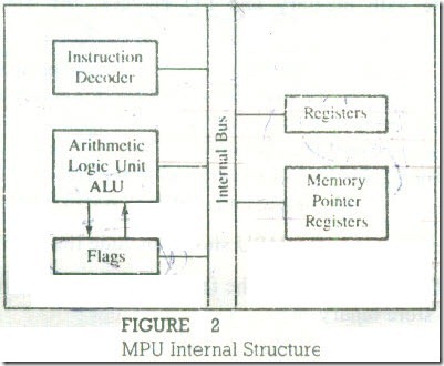
When the microprocessor executes instructions, it does so in a continuous sequence of fetch, decode, and execute operations. After examining these operations in more detail, we can describe the requirements of the internal architecture of our generalized microprocessor.
FETCHING AN INSTRUCTION
To fetch an instruction, the microprocessor places a memory address on the address bus and reads binary information using the data bus .Therefore, it needs a register that can hold memory addresses and increment these addresses after the fetching is completed, a sort of memory pointer.
DECODING AN INSTRUCTION
Once an instruction byte is fetched,' it needs to be decoded to answer the following:
· Is it a complete instruction? If not, how many more bytes need to be fetched?
· What type of operation is required and on what data ?
To perform these functions. the microprocessor needs an instruction decoder that can interpret the fetched binary information.
STORING DATA
The microprocessor gets data from memory, I/O, or directly as part of an instruction. Therefore. it needs a set of registers to store data (or addresses) temporarily before it can process the data.
EXECUTING AN INSTRUCTION
The type of data manipulation the microprocessor can perform depends on its internal micro programs , that is, on its instruction SCI. These operations can be classified as data copy (transfer). arithmetic/logic operations, and decision making .For example. to subtract two numbers, both numbers must be loaded into registers. After the subtraction, it is necessary to indicate whether the result is positive, negative, or zero. This can be indicated by setting or resetting flip-flops called flags. To perform these arithmetic and logic operations. the microprocessor needs a group of logic circuits called Arithmetic/Logic Unit (ALU).
This description of the requirements of the microprocessor to process data
FIGURE 2
MPU Internal Structure
can be summarized in a simplified block diagram shown in Figure 2 From this block diagram, we can derive a programming model for a specific microprocessor.
Review of Important Concepts
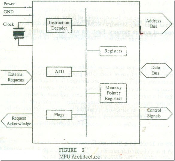
The description and the requirements of a generalized microprocessor unit can be summarized as follows
FIGURE 3
To communicate with memory and I/O devices, the MPU should have the following:
l. Address bus to send the address of a memory register or an I/O.
2. Data bus to transfer data between the MPU and memory and I/O devices.
3. Control signals to identify its operations and provide timing .
4. External Request signal lines to interrupt the MPU operations.
5. Request Acknowledge signals to respond to the requests by peripherals.
6. Clock signal to provide timing and power to operate circuits.
To process data internally, the MPU should include the following:
1. Instruction Decoder to decode the fetched binary information.
2. Registers to store binary data.
3. Registers as memory pointers for addressing memory registers.
4. ALU to perform arithmetic and logic operations.
5. Flags (flip-flops) to indicate data conditions for decision making.


Comments
Post a Comment