Posts

Showing posts with the label DESIGN OF COMPUTER INSTRUCTION SET AND THE CPU

QUESTIONS AND PROBLEMS

Image
QUESTIONS AND PROBLEMS 7.1 It is desired to implement the following instructions using block code: ADD, SUB, XOR, MOVE, HALT. Draw a block diagram. 7.2 The instruction length and the size of an address field are 9 bits and 3 bits respectively. Is it possible to have 6 two-address instructions 15 one-address instructions 8 zero-address instructions using expanding op-code technique? Justify your answer. 7.3 Using the instruction format of Problem 7.2, is it possible to have 7 two-address instructions 7 one-address instructions 8 zero-address instructions using expanding opcode technique? Justify your answer. 7.4 Assume that it is desired to have 2 two-address, 7 one-address, and 25 zero­ address instructions in a computer instruction set. Using expanding op-code technique with a 2-bit op-code and 3-bit address field, is it possible to accomplish the above? If so, justify your answer and determine the instruction length. 7.5 Assume that using an instructio...

Design of a Microprogrammed CPU

Image
7.4 Design of a Microprogrammed CPU Next, the design of a microprogrammed processor is illustrated. The programming model of this processor is shown in Figure 7.52. The CPU contains two registers: 1. An 8-bit register A                               2. A 2-bit flag register F The flag register holds only zero (Z) and carry (C) flags. All programs and data are stored in the 256 x 8 RAM. The detailed hardware schematic of the data-flow part of this processor is shown in Figure 7.53. From Figure 7.53, it can be seen that the hardware organization includes four more 8-bit registers, PC, IR, MAR, and BUFFER. These registers are transparent to a programmer. The 8-bit register BUFFER is used to hold the data that is retrieved from memory. In this system, only a restricted number of data paths are available. These paths are controlled by...

Microprogrammed Control Unit Design

Image
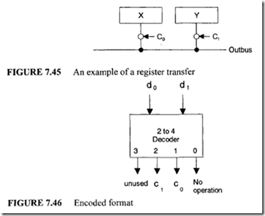
Microprogrammed Control Unit Design As mentioned earlier, a microprogramm d contwl unit contains programs written using microinstructions. These programs are stored in a control memory normally in a ROM inside the CPU. To execute instructions, the microprocessor reads (fetches) each instruction into the instruction register from external memory. The control unit translates the instruction for the microprocessor. Each control word contains signals to activate one or more microoperations. A program consisting of a set of microinstructions is executed in a sequence of micro-operations to complete the instruction execution. Generally, all microinstructions have two important fields: Control word Next address The control field indicates which control lines are to be activated. The next address field specifies the address of the next microinstruction to be executed. The concept of microprogramming was first proposed by W. V. Wilkes in 1951 utilizing a decoder an...

Alu design , design of the control unit , basic concepts and hardwired control design

Image
7.3.4 ALU Design Functionally, an ALU can be divided up into two segments: the arithmetic unit and the logic unit. The arithmetic unit performs typical arithmetic operations such as addition, subtraction, and increment or decrement by 1. Usually, the operands involved may be signed or unsigned integers. In some cases, however, an arithmetic unit must handle 4-bit binary-coded decimal (BCD) numbers and floating-point numbers. Therefore, this unit must include the circuitry necessary to manipulate these data types. As the name implies, the logic unit contains hardware elements that perform typical operations such as Boolean NOT and OR. In this section, the design of a simple ALU using typical combinational elements such as gates, multiplexers, and a 4-bit parallel adder is discussed. For this approach, an arithmetic unit and a logic unit are first designed separately; then they are combined to obtain an ALU. For the first step, a two-function arithmetic unit, as shown in Figure 7.2...