Summary of The internal hardware configuration of the 8051
Summary
The internal hardware configuration of the 8051 registers and control circuits have been examined at the functional block diagram level. The 8051 may be considered to be a collection of RAM, ROM, and addressable registers that have some unique functions.
SPECIAL-FUNCTION REGISTERS
| Register | Bit | Primary Function | Bit Addressable |
| A | 8 | Math, data manipulation | Y |
| B | 8 | Math | Y |
| PC | 16 | Addressing program bytes | N |
| DPTR | 16 | Addressing code and external data | N |
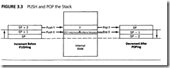
| SP | 8 | Addressing internal RAM stack data | N |
| PSW | 8 | Processor status | Y |
| P0-P3 | 8 | Store I/O port data | Y |
| TH0/TL0 | 8/8 | Timer/counter 0 | N |
| TH1/TL1 | 8/8 | Timer/counter 1 | N |
| TCON | 8 | Timer/counter control | Y |
| TMOD | 8 | Timer/counter control | N |
| SBUF | 8 | Serial port data | N |
| SCON | 8 | Serial port control | Y |
| PCON | 8 | Serial port control. user flags | N |
| IE | 8 | Interrupt enable control | Y |
| IP | 8 | Interrupt priority control | Y |
| DATA AND PROGRAM MEMORY | ||||
| Internal |
| Bytes | Function |
|
| RAM |
| 128 | RO- R7 registers, data storage, stack |
|
| ROM |
| 4K | Program storage |
|
| External |
| Bytes | Function |
|
| RAM |
| 64K | Data storage |
|
| ROM |
| 64K | Program storage |
|
EXTERNAL CONNECTION PINS
Function
Port pins 36 I/O, external memory, interrupts
Oscillator 2 Clock
Power 2

Comments
Post a Comment